1. OverviewThis paper looks at the success of the widely adopted PCI bus and describes a higher performance next generation of I/O interconnect technology – PCI Express – that will serve as a standard local I/O bus for a wide variety of future computing platforms. The paper also offers a technical overview of the evolution of PC buses, the physical and software layers of PCI Express, the benefits of PCI Express, and the implications this exciting new technology will have on measurement and automation systems. 2. PC HistoryWhen the PCI bus was first introduced in the early 1990s, it had a unifying effect on the plethora of I/O buses available on PCs at that time, such as VESA local bus, EISA, ISA, and Micro Channel, as shown in Figure 1. It was first implemented as a chip-to-chip interconnect and a replacement for the fragmented ISA bus. During these early years, the 33 MHz PCI bus was a good match for I/O bandwidth requirements of mainstream peripherals available at the time. Today, however, the story is quite different. Processor and memory frequencies have increased dramatically, with processor speeds increasing at the most aggressive rate. Over the intervening period, the PCI bus has increased in frequency from 33 to 66 MHz while processor speeds have increased from 33 MHz to 3 GHz. Emerging I/O technologies such as Gigabit Ethernet and IEEE 1394B can monopolize nearly all of the available PCI bus bandwidth as a single device on the bus.
3. PCI Bus History and OverviewThe PCI bus brought a number of advantages over previous bus implementations. Among the most important were processor independence, buffered isolation, bus mastering, and true plug-and-play operation. Buffered isolation essentially isolates, both electrically and by clock domains, the CPU local bus from the PCI bus. This feature brings two main benefits to system performance. The first is the ability to run concurrent cycles on the PCI bus and CPU bus; the second allows an increase in the CPU local bus frequency, independent of the PCI bus speed and loading. With bus mastering, PCI devices can gain access to the PCI bus through an arbitration process and master the bus transaction directly, as opposed to waiting for the host CPU to service the device, which results in a reduction of overall latency on servicing I/O transactions. Finally, plug-and-play operation, which permits devices to be automatically detected and configured, eliminated the manual setting of switches and jumpers for base address and DMA interrupts that frustrated users of ISA-based boards. 4. PCI ChallengesAlthough PCI has enjoyed great success, it now faces a series of challenges, including bandwidth limitations, host pin-count limitations, lack of real-time data transfer services such as isochronous data transfers, and features required for next-generation I/O requirements such as quality of service, power management, and I/O virtualization. Since the introduction of PCI, there have been several revisions to the PCI specification in order to keep up with the ever increasing I/O demands. These are summarized in Table 1. PCI Bus The usable bandwidth of the PCI bus and its derivatives can be significantly less than the theoretical bandwidth due to protocol overhead and bus topology. On the PCI bus, the available bandwidth is shared by all devices on the bus, resulting in lower bandwidth available per device as more devices are added. As PCI clock frequencies have become inadequate in certain applications, the PCI derivatives such as PCI-X and Advanced Graphics Port (AGP) have sought to provide bandwidth relief by increasing bus frequencies. A side effect of increasing frequencies is a commensurate reduction in the distance the bus can be routed and the number of connectors the bus transceivers can drive, which leads to the concept of dividing the PCI bus into multiple segments. Each of these segments requires a full PCI-X bus to be routed from the host driving silicon to each active slot. For example, the 64-bit PCI-X requires 150 pins for each segment. Clearly this is costly to implement and places strain on routing, board layer count, and chip package pin-outs. This extra cost is justified only where the bandwidth is crucial, such as in servers. Applications such as data acquisition, waveform generation, and multimedia applications including streaming audio and video require guaranteed bandwidth and deterministic latency, without which the user experiences glitches. The original PCI specification did not address these issues because the applications were not prevalent at the time the specification was developed. Today’s isochronous data transfers, such as high-definition uncompressed video and audio, demonstrate the need for the I/O system to include isochronous transfers. A side effect of isochronous transfers is that the local PCI Express devices need a lot less memory for buffering purposes than typical PCI devices use for minimizing variable bandwidth issues. Finally, next-generation I/O requirements such as quality of service measurements and power management will improve data integrity and permit selective powering-down of system devices – an important consideration as the amount of power required by modern PCs continues to grow. Virtual channels permit data to be routed via virtual routes; data transfers will take place even if other channels are blocked by outstanding transactions. Some of these features require software control beyond traditional PCI requirements and will not be available until OS and device driver support is available. Although the PCI bus is showing signs of age in some areas, the transition to PCI Express will be a long one, and the PCI bus will remain a strong contender for I/O expansion for many years to come. Modern PCs introduced in 2004 and later will have a combination of PCI and PCI Express slots, with the ratio increasingly favoring PCI Express as the technology is adopted. 5. PCI Express ArchitectureThe PCI Express architecture is specified in layers, as shown in Figure 2. Compatibility with the PCI addressing model (a load-store architecture with a flat address space) is maintained to ensure that all existing applications and drivers operate unchanged. The PCI Express configuration uses standard mechanisms defined in the PCI plug-and-play specification. The software layers will generate read and write requests that are transported by the transaction layer to the I/O devices using a packet-based, split-transaction protocol. The link layer adds sequence numbers and CRC to these packets to create a highly reliable data transfer mechanism. The basic physical layer consists of a dual simplex channel implemented as a transmit pair and a receive pair. The transmit and receive pair together are called a lane. The initial speed of 2.5 Gb/s provides a nominal bandwidth of about 250 MB/s in each direction per PCI Express lane. Once overhead is taken into account, about 200 MB/s of this is usable by the device for data movement. This rate represents a twofold to fourfold increase over most classic PCI devices. And unlike PCI, where the bus bandwidth was shared among devices, this bandwidth is provided to each device.
5a. Physical LayerThe fundamental PCI Express link consists of two low-voltage AC-coupled differential pairs of signals (a transmit pair and a receive pair) as shown in Figure 3. The physical link signal uses a de-emphasis scheme to reduce intersymbol interference, thus improving data integrity. A data clock is embedded using the 8b/10b encoding scheme to achieve very high data rates. The initial signaling frequency is 2.5 Gb/s/direction (Generation 1 signaling) and this is expected to increase in line with advances in silicon technology to 10 Gb/s/direction (the practical maximum for signals in copper). The physical layer transports packets between the link layers of two PCI Express agents.
The bandwidth of a PCI Express link may be linearly scaled by adding signal pairs to form multiple lanes. The physical layer provides x1, x2, x4, x8, x12, x16, and x32 lane widths, which conceputally splits the incoming data packets among these lanes. Each byte is transmitted, with 8b/10b encoding, across the lane(s). This data disassembly and reassembly is transparent to other layers. During initialization, each PCI Express link is set up following a negotiation of lane widths and frequency of operation by the two agents at each end of the link. No firmware or OS software is involved. The PCI Express architecture provides for future performance enhancements via speed upgrades and advanced encoding techniques. The future speeds, encoding techniques, or media would impact only the physical layer. The use of different lane widths in PCI Express requires the user to be attentive to the width required by an expansion board compared and to match that to the lane width provided by the motherboard. Other than graphics boards, which tend to be x16, many early PCI Express expansion boards will use the x1 width. As higher bandwidth is required, more boards will use the wider widths. Initial PCI Express computers offer an x16 connector as well as some combination of x1, x4, and x8 slots, depending on the intended market for the computer. PCI Express tolerates some interoperability between mismatched lane widths, depending on the direction of the mismatch. Using a larger-width expansion board in a smaller-width connector is referred to as down-plugging. For example, with PCI, you can insert a 64-bit PCI board in a 32-bit slot. In PCI Express, however, down-plugging is physically prevented by the design of the expansion board and connectors. The other mismatch – using a smaller-width expansion board in a larger-width connector – is up-plugging. Up-plugging is allowed, but with the caveat that the motherboard vendor is required to support the expansion board at only a x1 data rate while in this configuration, potentially wasting the investment in the expansion board with the faster interface. Whether a particular motherboard can handle an expansion board at its full data rate in an up-plugged configuration must be confirmed on a case-by-case basis with the motherboard manufacturer. For example, some motherboards can handle a x4 expansion board at its full x4 data rate when plugged into a x8 or x16 slot while other motherboards from the same vendor might run the board only at x1. In the case where a motherboard has both an integrated (onboard) graphic controller and an x16 PCI Express slot for future graphics expansion, it is normally not possible to use that x16 slot at the same time as onboard graphics are enabled. 5b. Data Link LayerThe primary role of a link layer is to ensure reliable delivery of the packet across the PCI Express link(s). The link layer is responsible for data integrity and adds a sequence number and a CRC to the transaction layer packet as shown in Figure 4. Most packets are initiated at the transaction layer. A credit-based, flow control protocol ensures that packets are transmitted only when it is known that a buffer is available to receive this packet at the other end, which eliminates any packet retries and the associated waste of bus bandwidth due to resource constraints. The link layer will automatically retry a packet that was signaled as corrupted.
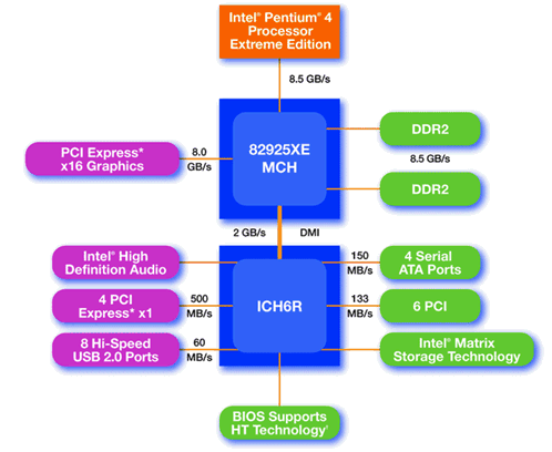
5c. Transaction LayerThe transaction layer receives read and write requests from the software layer and creates request packets for transmission to the link layer. All requests are implemented as split transactions and some of the request packets require a response packet. The transaction layer also receives response packets from the link layer and matches these with the original software requests. Each packet has a unique identifier that enables response packets to be directed to the correct originator. The packet format offers 32-bit memory addressing and extended 64-bit memory addressing. Packets also have attributes such as “no-snoop,” “relaxed ordering,” and “priority,” which may be used to route these packets optimally through the I/O subsystem. The transaction layer provides four address spaces – three PCI address spaces (memory, I/O and configuration) and message space. PCI 2.2 introduced an alternate method of propagating system interrupts called message signaled interrupt (MSI). Here a special-format memory-write transaction was used instead of a hard-wired sideband signal, as an optional capability in a PCI 2.2 system. The PCI Express specification reuses the MSI concept as a primary method for interrupt processing and uses a message space to accept all prior sideband signals, such as interrupts, power-management requests, and resets, as in-band messages. Other “special cycles” within the PCI 2.2 specification, such as interrupt acknowledge, are also implemented as in-band messages. You could think of PCI Express messages as “virtual wires” because their effect is to eliminate the wide array of sideband signals currently used in a platform implementation. 5d. Software LayerSoftware compatibility is of paramount importance for PCI Express. There are two facets of software compatibility – initialization (or enumeration) and run time. PCI has a powerful initialization model where the OS can discover all of the add-in hardware devices present and then allocate system resources, such as memory, I/O space, and interrupts, to create an optimal system environment. The PCI configuration space and the programmability of I/O devices are key concepts that remain unchanged within the PCI Express architecture; in fact, all OSs are able to boot without modification on a PCI Express-based machine. The run-time software model used by PCI is a load-store, shared-memory model, which is maintained within the PCI Express architecture to enable all existing software to execute unchanged. New software can also take advantage of some of the more advanced features of PCI Express, such as advanced switching, that are not covered in this paper. 6. PC Architecture – Today and FuturePC Architecture in 2002 with PCIThe PC architecture in 2002 consisted of a number of diverging requirements for each of the interconnects. For instance, graphics boards were interfaced via the advanced graphics port (AGP), and the memory bridge was connected to the I/O bridge via a number of interfaces, such as HubLink, as illustrated in Figure 5.
PC Architecture with PCI ExpressAs shown in Figure 6, PCI Express unifies the I/O system using a common bus architecture. In addition, PCI Express also replaces some of the internal buses that link subsystems.
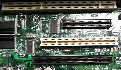
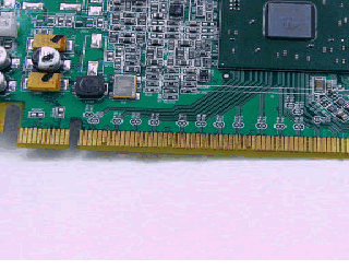
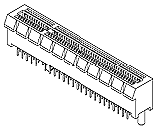
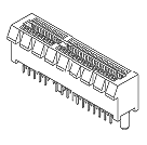
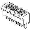
7. PCI Express PackagingPCI Express is available in a number of different I/O expansion formats, depending on the application platform – notebook, desktop, or server. Servers, which require larger bandwidths to service I/O requirements, will have more PCI Express slots, and these slots will provide higher PCI Express lane counts. In contrast, a notebook may use the PCI Express architecture internally, but provide only a single x1 lane for medium speed peripherals. 7a. Desktop PCI Express Expansion SlotsThe replacement for the PCI board for desktop and workstation machines will have a very similar mechanical structure to today’s PCI boards, based on a board-edge connector and retaining bracket with I/O connectors protruding through the bracket and attached to the main PWB. The connector on the motherboard has improved retention capabilities, to ensure that the board will not become dislodged from the connector under vibration or during shipping. The board-edge connector is available in a number of different sizes, depending on PCI Express lane width, from x1 up to x16. It is planned for the x16 to replace the AGP slot on motherboards, for graphics board expansion. Figure 7 shows a photo of a motherboard with four slots – one PCIe x16, one PCI, one PCIe x8, and one PCI-X (from bottom to top). Note that the motherboard still has classic PCI slots, and the classic PCI slots will probably be available for a long time. Figure 8 shows a photo of a typical graphics board, featuring an x16 link and the potential to move data at 3.2 GB/s. Figure 9 shows a mechanical drawing for various PCI Express connectors.
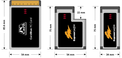
Figure 9. Mechanical Drawings of Various PCI Express Connectors 7b. ExpressCardThe ExpressCard standard gives users a very easy way to add hardware or media to their systems. The primary market for ExpressCard modules are notebooks and small PCs needing only limited expansion. The ExpressCard module can be plugged in or removed at almost any time without any tools (unlike traditional add-in boards for desktop computers). ExpressCard technology provides desktop and mobile computer users a consistent, easy, and reliable way to connect devices into their systems. ExpressCard technology replaces conventional parallel buses for I/O devices with two scalable, high-speed serial interfaces – PCI Express and USB 2.0. ExpressCard developers can create modules using PCI Express for their highest-performance applications or use USB to take advantage of the wide variety of USB silicon already available. Irrespective of the bus technology that the module vendor chooses, the end user experience will be the same. There will be no external indications to the end user of which underlying bus the module is using. There are two standard formats for ExpressCard modules – ExpressCard/34 (34 mm wide) and ExpressCard/54 (54 mm wide). Both modules are 5 mm thick, the same as the Type II PC Card. The standard module length is 75 mm, which is 10.6 mm shorter than a standard PC Card. Both the ExpressCard/34 and ExpressCard/54 modules use the same connector interface. The two sizes of ExpressCard modules give system manufacturers a degree of flexibility that they did not have with earlier module standards. While the ExpressCard/34 device is better suited to smaller systems, the wider ExpressCard/54 module can accommodate devices that will not physically fit into the narrower ExpressCard/34 format. Figure 10 shows the two ExpressCard modules sizes and contrasts them to the PCMCIA CardBus module. Examples of the larger ExpressCard/54 modules include SmartCard readers, Compact Flash readers, and 1.8 in. disk drives. In addition to providing extra space for components, the ExpressCard/54 module also dissipates more thermal energy than the smaller ExpressCard/34 module. This feature may make ExpressCard/54 a natural choice for higher-performance and first-generation applications. However, a module manufacturer who can fit an application into the narrow module will have an advantage in that the module will work in both sizes of ExpressCard slots. To improve the ease of use, the ExpressCard/54 slot includes a guidance feature designed to steer ExpressCard/34 modules easily into the connector socket. It is also worth pointing out that the dimensions are such that inserting a CardBus card into an ExpressCard slot or vice versa will not damage either part. Each slot of the ExpressCard host interface must include a single PCI Express lane (x1) operating at the baseline 2.5 Gb/s data rate, in each direction, as defined by the PCI Express Base Specification 1.0a. The ExpressCard host interface must also accept the low, full, and high-speed USB data rates as defined by the USB 2.0 Specification. Providing both interfaces is a condition for being an ExpressCard-compliant host platform. An ExpressCard module can use one or both of the standard interfaces depending on the application requirements. 7c. Server I/O ModulesServers need I/O adapter packaging that addresses items such as closed-chassis adapter removal/insertion, integrated hot-plug, adapter protection from ESD and handling damage, standardized management interfaces and features, adequate cooling, single bulk power supply, and reduced I/O footprint in servers. The Server I/O Module (SIOM) specification defines two PCI Express modular packages for I/O adapters, which are designed to provide closed-chassis installation and removal. They are also designed for native hot-plug, meaning that no damage will occur to the module or chassis from installing or removing the modules while the chassis is powered. The two formats, identical in height and depth, vary only by the width or slot space they consume in the chassis. The single-wide module will fit in any SIOM slot. The double-wide module requires two adjacent SIOM slots. A single-wide module can have up to an x8 PCI Express connection; a double-wide module can offer up to an x16 connection. (Double-wide slots are optional in PCI Express SIOM servers.) A minimum management interface, standard on all modules, consists of an EEPROM that provides management data about the adapter to the host system. An optional internal storage interface accepts up to four x1 ports of SAS/SATA and a sideband interface for controlling drive LEDs. SIOMs and SIOM chassis share requirements for cooling. SIOM chassis are required to provide a minimum airflow to each slot as defined by this specification. SIOMs are required to provide a minimum and maximum airflow resistance to ensure that the SIOM will have a defined airflow for I/O cooling and that I/O thermal load is not added to the chassis. 8. Benefits of PCI ExpressFor PC-based measurement and automation systems, the PCI bus has been the bus of choice for plug-in expansion boards for many years. It will continue to play an important role in the future. As the PC has evolved, the PCI bus (with its parallel architecture) has not scaled linearly with the rest of the platform. PCI Express answers these issues and provides benefits across five main areas: * High Performance – relates specifically to bandwidth, which is more than double that of PCI in an x1 link, and grows linearly as more lanes are added. An additional benefit that is not immediately evident is that this bandwidth is simultaneously available in both directions on each link. In addition, the initial signaling speed of 2.5 Gb/s is expected to increase, yielding further speed improvements. All of these features will ensure that the PC evolves into an increasingly attractive platform on which to base next-generation measurement and automation systems. Glossary8b/10b Encoding – A scheme for encoding signals with an embedded clock. The encoding serves two purposes. First, it ensures that there are enough transitions in the data stream for clock recovery and second, that the number of 0s and 1s is matched, maintaining DC balance in AC-coupled systems. AGP – Advanced Graphics Port – a higher-speed version of the PCI bus using a different connector. Developed to accommodate the bandwidth needs of dedicated plug-in graphics cards in desktop PCs. CRC – Cyclic Redundancy Check – a method of detecting and correcting bit errors in a packet of information by adding a calculated set of values to the packet. The values are derived from an original packet of data. Differential – Differential signaling uses two wires carrying a signal which is 180 deg out of phase. The main benefit is a reduction in susceptibility to induced noise. ExpressCard – A small I/O card including both PCI Express and USB 2.0 interfaces. ISA Bus – Industry Standard Architecture – a bus standard for PCs introduced in 1984 that extended the XT bus architecture to 16 bits. It is designed to connect peripheral cards to the motherboard. It is also referred to as the AT bus. PICMG – PCI Industrial Computer Manufacturers Group – the group of member companies that maintains current specifications for CompactPCI and PCI/ISA. PCI – Peripheral Component Interconnect – a high-speed parallel bus originally designed by Intel to connect I/O peripherals to a CPU. PCI Express – An evolutionary version of PCI that maintains the PCI software usage model and replaces the physical bus with a high-speed (2.5 Gb/s) serial bus serving multiple lanes. SIOM – Server I/O Module – an I/O module, designed for server and workstation applications, that uses PCI Express for communication. USB 2.0 – USB 2.0 is an external differential point-to-point serial bus that provides data rates up to 480 Mb/s. USB 2.0 is an extension of USB 1.1 that uses the same cables and connectors |
Feedback |
| If you have any suggestion/feedback please email it to [email protected] |


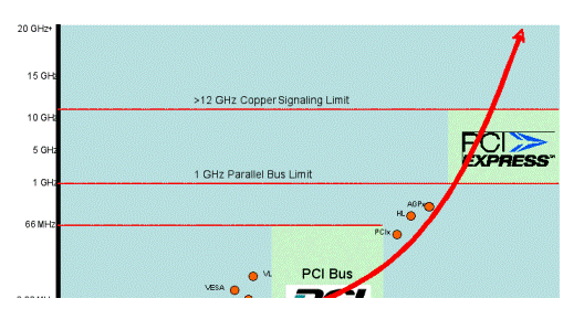
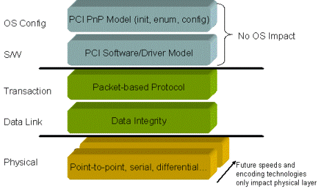
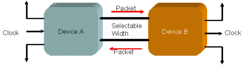
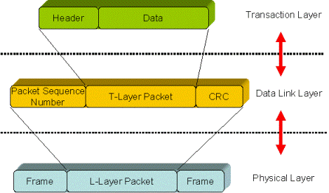
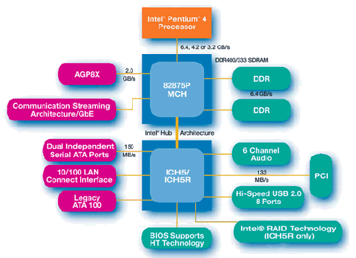 Figure 5. PC Architecture in 2002 with PCI (courtesy of Intel)